Competitive PCB Manufacturer

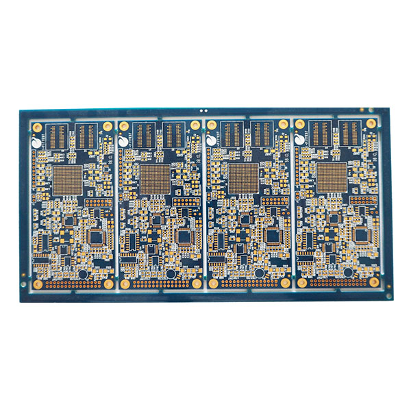
Resin plugging hole Microvia Immersion silver HDI with laser drilling
Material type: FR4
Layer count: 4
Min trace width/space: 4 mil
Min hole size: 0.10mm
Finished board thickness: 1.60mm
Finished copper thickness: 35um
Finish: ENIG
Solder mask color: blue
Lead time: 15 days
From the 20th century to the beginning of the 21st century, the circuit board electronics industry is druing the rapid development period of technology, electronic technology has been rapidly improved. As a printed circuit board industry, only with its synchronous development, can constantly meet the needs of customers. With the small, light and thin volume of electronic products, the printed circuit board has developed flexible board, rigid flexible board, blind buried hole circuit board and so on.
Talking about blinded/buried holes, we start with traditional multilayer . The standard multi-layer circuit board structure is composed of inner circuit and outer circuit, and the process of drilling and metalization in the hole is used to achieve the function of internal connection of each layer circuit. However, due to the increase of line density, the packaging mode of parts is constantly updated. In order to make the circuit board area limited and allow for more and higher performance parts, in addition to the thinner line width, the aperture has been reduced from 1 mm of DIP jack aperture to 0.6 mm of SMD, and further reduced to less than 0.4mm. However, surface area will still be occupied, so buried hole and blind hole can be generated. The definition of buried hole and blind hole is as follows:
Buired hole:
The through hole between the inner layers, after pressing, cannot be seen, so it does not need to occupy the outer area, the upper and lower sides of the hole are in the inner layer of the board, in other words, buried in the board
Blinded hole:
It is used for the connection between the surface layer and one or more inner layers. One side of the hole is on one side of the board, and then the hole is connected to the inside of the board.
The advantage of the blinded and buried hole board:
In non-perforating hole technology, the application of blind hole and buried hole can greatly reduce the size of PCB, reduce the number of layers, improve the electromagnetic compatibility, increase the characteristics of electronic products, reduce the cost, and also make the design work more simple and fast. In traditional PCB design and processing, through-hole can cause many problems. Firstly, they occupy a large amount of effective space. Secondly, a large number of through-holes in a dense area also cause great obstacles to the wiring of the inner layer of multi-layer PCB. These through-holes occupy the space needed for wiring, and they densely pass through the surface of the power supply and ground wire layer, which will destroy the impedance characteristics of the power supply ground wire layer and cause the failure of the power supply ground wire layer. And conventional mechanical drilling will be 20 times as much as the use of non-perforating hole technology.
PRODUCT CATEGORIES
Focus on providing mong pu solutions for 5 years.